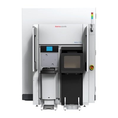
Thermo Scientific Helios 5 PXL PFIB Wafer DualBeam Enables Inline Metrology of Advanced 3D Structures

HILLSBORO, Ore., Feb. 16, 2021 /PRNewswire/ — Thermo Fisher Scientific, the world leader in serving science, today launched the Thermo Scientific Helios 5 PXL PFIB Wafer DualBeam. The system, a plasma focused ion beam scanning electron microscope, reduces time-to-data from days to hours for inline through-stack metrology and verification of high-aspect ratio structures.
The Helios 5 PXL offers high-resolution, high-contrast imaging as well as fast, precise, large-area sample deprocessing, diagonal milling and cross sectioning of advanced 3D semiconductor devices, such as 3D NAND and advanced memory. The easy-to-use system supports whole wafer analysis and fully automates delayering, milling and metrology in the fab, reducing wafer scrap while accelerating yield learning.
“As layer counts increase, the manufacturing process for current and future high-aspect-ratio structures is becoming increasingly complex,” said Glyn Davies, vice president and general manager of semiconductor at Thermo Fisher. “With this breakthrough system, already being used by a global leader in semiconductor manufacturing, high-volume fabrication customers will be able to measure thousands of metrology points at multiple positions in the 3D stack for high aspect ratio and buried structures.”
The new Helios 5 PXL enables full inline metrology and process monitoring for advanced process control and excursion monitoring compliant with latest 300mm fab communication protocols and standards. Users can reliably measure and verify features of interest within complex vertical stacks and high-aspect ratio structures.
Other benefits of the Helios 5 PLX include:
- Nanometer-scale SEM imaging;
- High-volume, high-speed milling and cross sectioning;
- Optimized planar deprocessing for high sensitivity materials and surface quality preservation;
- Deprocessing of advanced metallization layers through proprietary chemistries;
- Precise, site-specific preparation of large-area lamellae with the optional Thermo Scientific EasyLift Nanomanipulator; and
- Full coverage of 300 wafer handling.
To learn more about the Helios 5 PXL, visit https://ter.li/Helios5PXL.
About Thermo Fisher Scientific
Thermo Fisher Scientific Inc. is the world leader in serving science, with annual revenue exceeding $30 billion. Our Mission is to enable our customers to make the world healthier, cleaner and safer. Whether our customers are accelerating life sciences research, solving complex analytical challenges, improving patient diagnostics and therapies or increasing productivity in their laboratories, we are here to support them. Our global team of more than 80,000 colleagues delivers an unrivaled combination of innovative technologies, purchasing convenience and pharmaceutical services through our industry-leading brands, including Thermo Scientific, Applied Biosystems, Invitrogen, Fisher Scientific, Unity Lab Services and Patheon. For more information, please visit www.thermofisher.com.
Media Contact Information:
Kathy Gill
Thermo Fisher Scientific
+1 971-294-9262
kathy.gill@thermofisher.com
View original content to download multimedia:http://www.prnewswire.com/news-releases/thermo-scientific-helios-5-pxl-pfib-wafer-dualbeam-enables-inline-metrology-of-advanced-3d-structures-301228439.html
SOURCE Thermo Fisher Scientific

