Ansys Multiphysics Signoff Solutions Certified for Samsung’s 2nm Power Backside Delivery Technology

Certification of Ansys power integrity platforms includes revolutionary new technology for power distribution on advanced chips
/ Key Highlights
- Ansys RedHawk-SC™ and Ansys Totem™ power integrity platforms are certified for Samsung’s SF2Z manufacturing technology
- Ansys solutions enable early adopters to reliably design leading-edge semiconductor products for high-performance computing (HPC), smartphones, artificial intelligence (AI), data center communication, and graphics processors
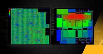
PITTSBURGH, June 26, 2024 /PRNewswire/ — Ansys (NASDAQ: ANSS) power integrity solutions have been certified by Samsung Foundry for use with Samsung’s new SF2Z 2nm gate-all-around manufacturing technology. SF2Z includes advanced technology that moves the power distribution network to the backside of the chip — saving space, lowering costs, and improving performance. Ansys solutions enable early adopters of Samsung’s technology to design leading-edge semiconductor products for HPC, smartphones, AI, data center communication, and graphics processors.
The certification includes RedHawk-SC, which provides predictively accurate signoff verification for electromigration and voltage drop (IR drop) on power distribution networks for digital designs. In addition, the Totem power integrity platform provides comprehensive evaluation for analog and mixed-signal designs. Both RedHawk-SC and Totem signoff capabilities can reduce project risk, improve reliability, and extend the longevity of chips.
“Samsung Foundry has worked very closely with Ansys for many years to ensure that our mutual customers have timely access to the design tools they need,” said Sangyun Kim, vice president of Foundry Design Technology Team at Samsung Electronics. “Our continued collaboration with Ansys is critical as we tackle new customer challenges in digital, full-custom, mixed-signal, and 3D-IC designs.”
“Ansys and Samsung are focused on delivering technology enablement solutions that meet our customers’ semiconductor technology needs,” said John Lee, vice president and general manager of the electronics, semiconductor, and optics business unit at Ansys. “This collaboration supports the fidelity of our Ansys multiphysics signoff platform and exemplifies Ansys’ commitment to powering the best user experience for our joint customers.”
/ About Ansys
Our Mission: Powering Innovation that Drives Human Advancement™
When visionary companies need to know how their world-changing ideas will perform, they close the gap between design and reality with Ansys simulation. For more than 50 years, Ansys software has enabled innovators across industries to push boundaries by using the predictive power of simulation. From sustainable transportation to advanced semiconductors, from satellite systems to life-saving medical devices, the next great leaps in human advancement will be powered by Ansys.
Ansys and any and all ANSYS, Inc. brand, product, service and feature names, logos and slogans are registered trademarks or trademarks of ANSYS, Inc. or its subsidiaries in the United States or other countries. All other brand, product, service and feature names or trademarks are the property of their respective owners.
ANSS–T
/ Contacts
|
Media |
Mary Kate Joyce |
|
724.820.4368 |
|
|
Investors |
Kelsey DeBriyn |
|
724.820.3927 |
|
![]() View original content to download multimedia:https://www.prnewswire.com/news-releases/ansys-multiphysics-signoff-solutions-certified-for-samsungs-2nm-power-backside-delivery-technology-302182556.html
View original content to download multimedia:https://www.prnewswire.com/news-releases/ansys-multiphysics-signoff-solutions-certified-for-samsungs-2nm-power-backside-delivery-technology-302182556.html
SOURCE Ansys


